Overview
The core facilities in Research Center of Applied Sciences (RCAS) provide assistances for the researchers to conduct various experiments in bio-image detection, material surface analysis, components structure production and micro sample fabrication.
All instruments are located on 6th, 4th and B2 floors in Interdisciplinary Research Building for Science and Technology (IRBST). Furthermore, several public laboratories on 6th, 4th and B2 floors in IRBST are established for our members to do researches in fabrication, imaging, cell and protein.
The RCAS core facilities can be divided into three categories by features: Microscope, Materials Analysis, Micro Fabrication.
| Type | Instruments | Features | Brand Model | Location |
|---|---|---|---|---|
| Microscope | Atomic force | microscope Material surface analysis | Bruker DM-CAFM | NCTU TKP 506 |
| Laser scanning Confocal Spectral Microscope | Bio and fluorescent sample detection | Leica TCS-SP5 | IRBST 4B20 | |
| Atomic force microscope | Bio materials and nano components detection | JPK Nano Wizard II & III | IRBST B2C01 | |
| High resolution Raman microscope | Fluorescence and crystallization analysis | Jobin Yvon HR800 | IRBST 6B08 | |
| Field emission scanning electron microscop | Analysis of surface morphology and elemental analysis | Nova 200 NPE 44/D8187 | IRBST 4C05 | |
| Materials Analysis | X-ray photo-electron spectroscope | Surface and Depth Analysis of Elementals | ULVAC-PHI PHI-5000 Versaprobe | IRBST 4C05 |
| Scanning Ion Microscope | Surface and Depth Analysis of Molecules and Atoms | ULVAC-PAI TRIFTV | IRBST 4C05 | |
| Time-resolved confocal microscope for single molecule spectrometer | Multi-Channel time resolve spectroscopy | PicoQuant Micro Time 2000 | IRBST 6B10 | |
| Variable angle spectroscopic ellipsometer | Material film thickness and refractive index analysis | VUV-VASE, Gen-II | IRBST 6A02 | |
| Color 3D Laser Scanning Microscope | Surface profile and roughness detection | Keyence VK9710K S/N 2190011 | IRBST 4C01 | |
| Benchtop maskless lithography system | Structure production of photoresist on components | Heidelberg uPG501 | IRBST B2C02 | |
| Micro Fabrication | Specimen Preparation Equipment | Thin-film growth and etching | Gated Sted SKE104005 | IRBST 6A02 |
| Focus Ion Beam | Stucture production of nano components | FEI NanoLab660 | IRBST 4B19 | |
| Inductively coupled plasma etching system | Dry and wet etching of nano components | OXFORD ICP65 | IRBST B2C02 |
we would upgrade the facilities and improve the laboratory configuration.
Moreover, we have suitable plan and management for every lab and instrument in safety considerations of research.
| Type | Instruments | Features | Brand Model | Location |
|---|---|---|---|---|
| Microscope | Atomic force | microscope Material surface analysis | Bruker DM-CAFM | NCTU TKP 506 |
| Laser scanning Confocal Spectral Microscope | Bio and fluorescent sample detection | Leica TCS-SP5 | IRBST 4B20 | |
| Atomic force microscope | Bio materials and nano components detection | JPK Nano Wizard II & III | IRBST B2C01 | |
| High resolution Raman microscope | Fluorescence and crystallization analysis | Jobin Yvon HR800 | IRBST 6B08 | |
| Field emission scanning electron microscop | Analysis of surface morphology and elemental analysis | Nova 200 NPE 44/D8187 | IRBST 4C05 | |
| Materials Analysis | X-ray photo-electron spectroscope | Surface and Depth Analysis of Elementals | ULVAC-PHI PHI-5000 Versaprobe | IRBST 4C05 |
| Scanning Ion Microscope | Surface and Depth Analysis of Molecules and Atoms | ULVAC-PAI TRIFTV | IRBST 4C05 | |
| Time-resolved confocal microscope for single molecule spectrometer | Multi-Channel time resolve spectroscopy | PicoQuant Micro Time 2000 | IRBST 6B10 | |
| Variable angle spectroscopic ellipsometer | Material film thickness and refractive index analysis | VUV-VASE, Gen-II | IRBST 6A02 | |
| Color 3D Laser Scanning Microscope | Surface profile and roughness detection | Keyence VK9710K S/N 2190011 | IRBST 4C01 | |
| Benchtop maskless lithography system | Structure production of photoresist on components | Heidelberg uPG501 | IRBST B2C02 | |
| Micro Fabrication | Specimen Preparation Equipment | Thin-film growth and etching | Gated Sted SKE104005 | IRBST 6A02 |
| Focus Ion Beam | Stucture production of nano components | FEI NanoLab660 | IRBST 4B19 | |
| Inductively coupled plasma etching system | Dry and wet etching of nano components | OXFORD ICP65 | IRBST B2C02 |
主要提供薄膜製程機台以協助本中心及本院同仁進行光電元件、量子元件、感測器及微流道等相關開發研究。

感應式耦合電漿蝕刻系統
Oxford ICP-RIE
- 薄膜蝕刻種類:非金屬
- 製程氣體:O2, CHF3
- 蝕刻真空度:1-10 mTorr
- 沈積時最低操作壓力:200-2000mTorr
- 電漿產生裝置:上電極:15V
下電極:-15V - 適用基板尺寸:4" wafer
- 使用費:1000/h

電子束蒸鍍系統
Ulvac E Beam Evaporator
(for
oxide)
- 蒸鍍材料種類:氧化物
- 蒸鍍源:可同時容納4個鍍源材料
- 製程氣體:O2
- 最低真空能力:~10-7 torr
- 操作壓力:5X10⁻⁶ torr
- 最高壓力:3X10⁻⁵ torr
- 極限加熱溫度:150 ℃
- 旋轉速率:15 rpm
- 適用基板尺寸:4" wafer
- 使用費:800/h

電子束蒸鍍系統
Ulvac E Beam Evaporator
(for
metal)
- 蒸鍍材料種類:金屬
- 蒸鍍源:可同時容納6個鍍源材料
- 最低真空能力:~10-7 torr
- 操作壓力:5X10⁻⁶ torr
- 最高壓力:3X10⁻⁵ torr
- 極限加熱溫度:150 ℃
- 旋轉速率:0-25 rpm
- 適用基板尺寸:4" wafer
- 使用費:800/h

熱蒸鍍系統
Ulvac Thermal Evaporator
- 蒸鍍材料種類:金屬、非金屬
- 蒸鍍源:可同時容納4個鍍源材料
2種材料同時共蒸鍍 - 極限壓力:~10-4 Pa
- 操作壓力:4X10⁻⁴ Pa(3X10⁻⁶ torr)
- 蒸鍍溫度:150 ℃
- 旋轉速率:non
- 適用基板尺寸:4" wafer
- 使用費:500/h

射頻/直流濺鍍系統
RF/DC Sputter
- 濺鍍材料種類:金屬、非金屬
- 蒸鍍源:2 DC-gun, 1 RF-gun
可同時1 DC 1 RF共濺鍍 - 靶材需求:3" target
- 製程氣體:Ar, O2
- 極限壓力:~10-6 torr
- 操作壓力:1-50 mTorr
- 旋轉速率:15 rpm
- 適用基板尺寸:4" wafer
- 使用費:500/h

直流濺鍍系統
DC Sputter
- 濺鍍材料種類:金屬
- 蒸鍍源:1 DC-gun/ 2 DC-gun
- 靶材需求:2"/3" target
- 製程氣體:Ar
- 極限壓力:~10-6 torr
- 操作壓力:1-50 mTorr
- 旋轉速率:
- 濺鍍溫度:non/700 ℃
- 適用基板尺寸:4" wafer
- 使用費:500/h

奈米壓印曝光機
Mask Aligner EVG620 NT
- 光源功率:
- 光源波長:
- 曝光強度:
- 適用基板尺寸:
- 使用費:1000/h

直寫機
Heidelberg direct writer
- 光源功率:70mW
- 光源波長:365nm
- 曝光強度:
- 適用基板尺寸:破片
2"-5"矽晶圓
2"-5"玻璃光罩 - 使用費:800/h


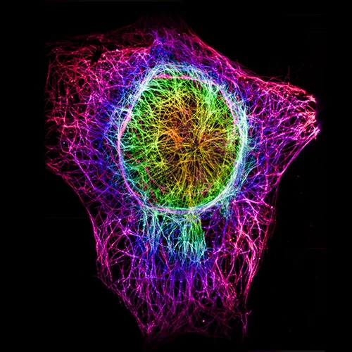
Lattice light sheet microscope
Related Research Results


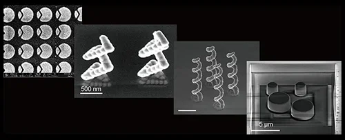
Scanning Ion Microscope
Related Research Results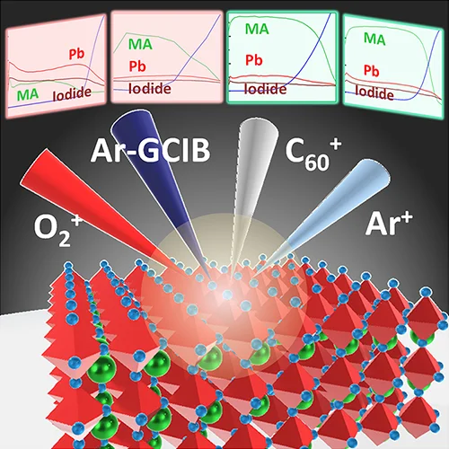
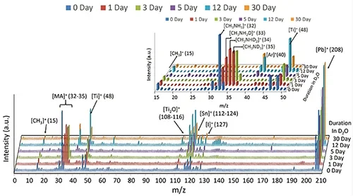


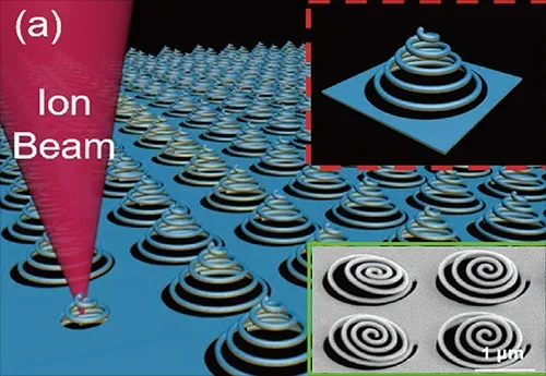
Focus Ion Beam
Related Research Results