The main objective of the Thematic Center for Quantum Photonics is
to develop key materials and devices for applications in photonic quantum
technologies. We synergize the existing research strengths in RCAS, including
material growth, spectroscopy measurements, device fabrications, and
theoretical analysis. Collaborations with domestic and overseas leading
research teams have also been established in order to leverage state-of-theart
techniques for tackling the technical barriers in materials and devices for
applications in quantum photonics technologies.
Research Areas
The research areas of the Thematic Center include:
(1) Developing quantum light source and single-photon detectors;
(2) exploring room-temperature quantum systems for applications in spin control and quantum sensing;
(3) design and fabrication of nanophotonic structures;
and (4) Developing emergent materials for new device architectures.
We hope in the long term can achieve significant breakthroughs in photonic quantum computations and communications.
Focusing project
Quantum Photonic Applications of Novel Materials
The emerging field of quantum technology has opened up new opportunities for the development of new optoelectronic devices. For future quantum technology, quantum photonic devices will play a crucial role in various aspects and bring revolutionary changes. This project aims at developing three critical areas including:
(1) Single-photon emitters with high brightness, efficiency, and indistinguishability.
(2) Superconducting single-photon detectors based on high-quality superconducting materials to achieve high sensitivity, fast response, high detection efficiency, and low noise.
(3) Quantum photonic chips and exploration of novel physical mechanisms to improve quantum photonic devices.
The developed quantum photonic devices will be the foundation for future developments in quantum information technology.
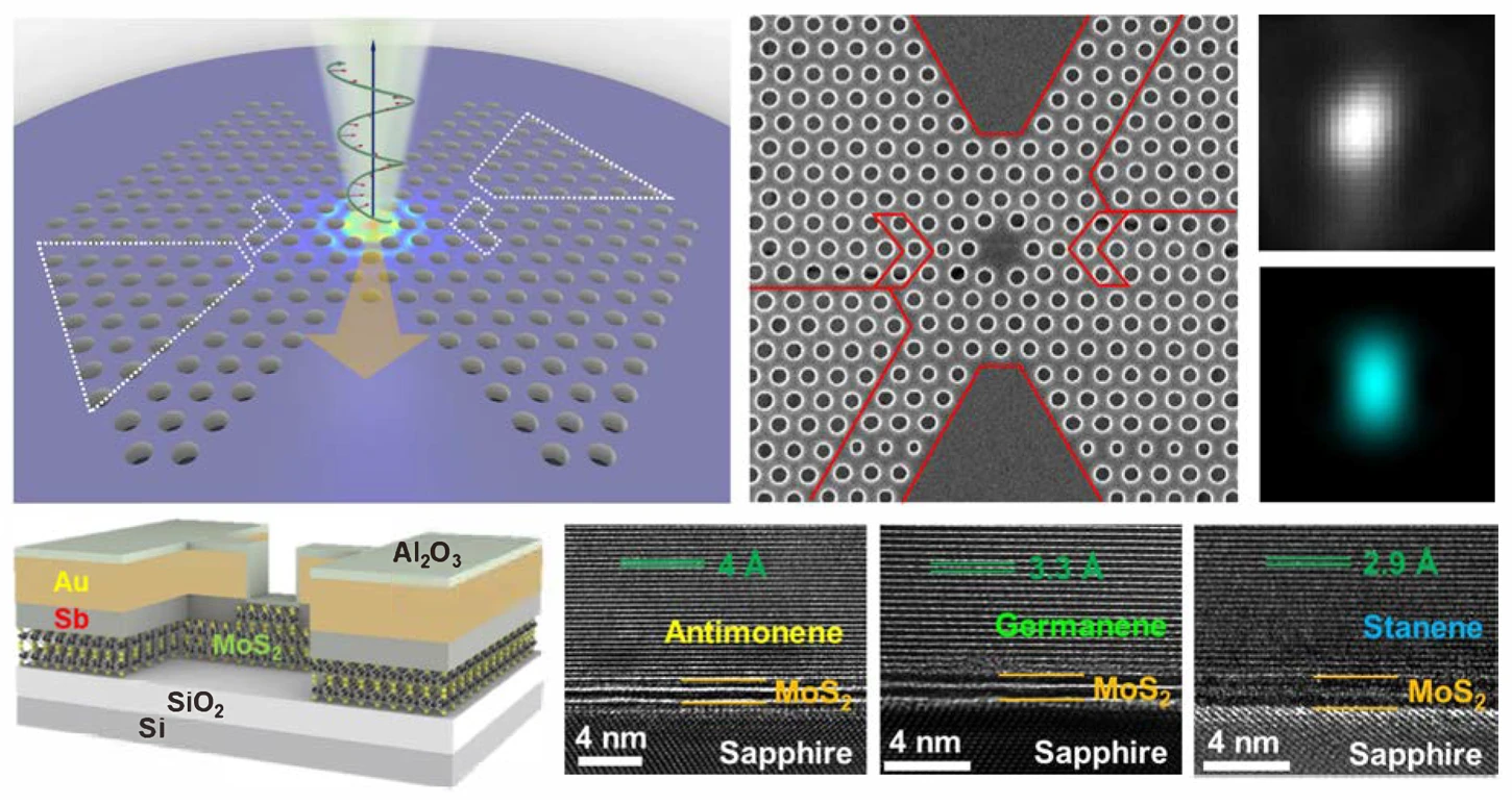
Photonic design for controlling emission of single photon emitter
Once the generic properties of a single photon emitter are known, the next step is to tailor its emission characteristics so that the emitted single photon can be utilized for quantum applications in successive systems. A few key features of the single photon could be manipulated at the emission stage, including the emission rate, emission direction, and polarization state of single photons. In this project, specialized photonic structures will be developed to control of single photon emissions, particularly focusing on the design of cavities, waveguide, and chiral structures that can enable manipulations of single photons.
Crystallinity of Electrodes: Extraction and Modelling of Contact Resistance on 2D Material Surfaces in the Nanometer Regime for Device Applications
The high contact resistance at electrodes and 2D material interfaces is one major bottleneck for further device performance improvement of 2D material devices. We have demonstrated that by using polycrystalline antimonene as the contact electrodes through traditional photolithography and metal lift-off procedures, reduced contact resistance and enhanced device performances can be observed. However, due to its weak thermal and chemical endurance, antimonene may not be a promising candidate as the contact electrodes in semiconductor fabrication lines. In our preliminary study, we have demonstrated that the crystallinity of the contact electrodes may be the major issue influencing the contact resistance at the metal/2D material interfaces. Therefore, the goal of this project is to explore the actual mechanism responsible for the reduced contact resistance at the metal/2D material interfaces with enhanced electrode crystallinity. To reduce the influence of channel resistance to the measurement results, conductive atomic force microscope will be adopted to extract the actual contact resistance of different contact metals in the nanometer regime. First-principles modelling will be performed to gain deeper understanding. We also explore the opportunity to apply the low-resistance contacts to the compact light-emitting devices.